


Spin-orbit torque (SOT) is widely considered as the key technology for next-generation magnetic random-access memory (MRAM), leveraging ultrafast operating speed and unlimited endurance. However, integrating perpendicular magnetic anisotropy (PMA) SOT-MRAM stacks with the back-end-of-line (BEOL) thermal budget remains a critical challenge, as PMA degradation and Pt-Fe interdiffusion typically occur under 400 °C annealing. Here we propose a double CoFeB reference layer (DCFB) structure to address these issues. The additional CoFeB reference layer and two extra CoFeB/W interfaces significantly enhance the PMA of the reference layers, while improving the crystallization of the overlying Pt/Co multilayers. Furthermore, the DCFB stack effectively acts as a diffusion barrier against Pt-Fe interdiffusion. Consequently, a fabricated magnetic tunnel junction (MTJ) incorporating the DCFB stack achieves a high tunneling magnetoresistance (TMR) of 137% even after annealing at 400 °C. Our work provides a robust, simplified approach for the design of SOT-MRAM stacks with BEOL thermal budget tolerance.
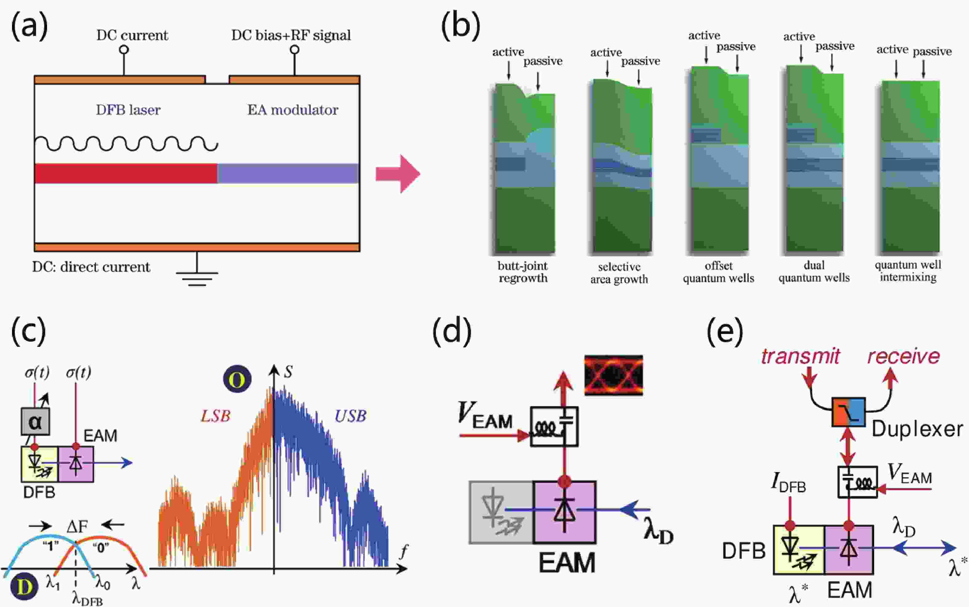
Currently, the global 5G network, cloud computing, and data center industries are experiencing rapid development. The continuous growth of data center traffic has driven the vigorous progress in high-speed optical transceivers for optical interconnection within data centers. The electro-absorption modulated laser (EML), which is widely used in optical fiber communications, data centers, and high-speed data transmission systems, represents a high-performance photoelectric conversion device. Compared to traditional directly modulated lasers (DMLs), EMLs demonstrate lower frequency chirp and higher modulation bandwidth, enabling support for higher data rates and longer transmission distances. This article introduces the composition, working principles, manufacturing processes, and applications of EMLs. It reviews the progress on advanced indium phosphide (InP)-based EML devices from research institutions worldwide, while summarizing and comparing data transmission rates and key technical approaches across various studies.

A skipper image sensor (SIS) with lateral overflow gate-coupled capacitor (LOGCC) is proposed in this work. During the integration period, the transfer gates after TG are switched on to construct a LOGCC with specific operation timing. Once high light illumination fully charges the pinned photodiode (PPD), the extra photogenerated electrons will overflow to LOGCC, which effectively improve the dynamic range (DR) of SIS. Before the readout of signal in PPD, the electrons stored in LOGCC are sampled and then reset through the floating diffusion (FD). In the end, the electrons in PPD are sampled by the method of the conventional skipper pixels. According to TCAD simulation results, the extra electrons are transferred to LOGCC through the TG effectively. Measurement of prototype chip shows that the DR is extended to 89.3 dB. As contrast, the DR is 66 dB when switching off the transfer gates, i.e. LOGCC. Compared with traditional SIS, the proposed architecture achieved DR extension by introducing LOGCC which is constructed with transfer gates. Therefore, this study proposes the introduction of LOGCC to expand the application scenarios of SIS, providing a new approach for its use in conditions requiring stronger light.


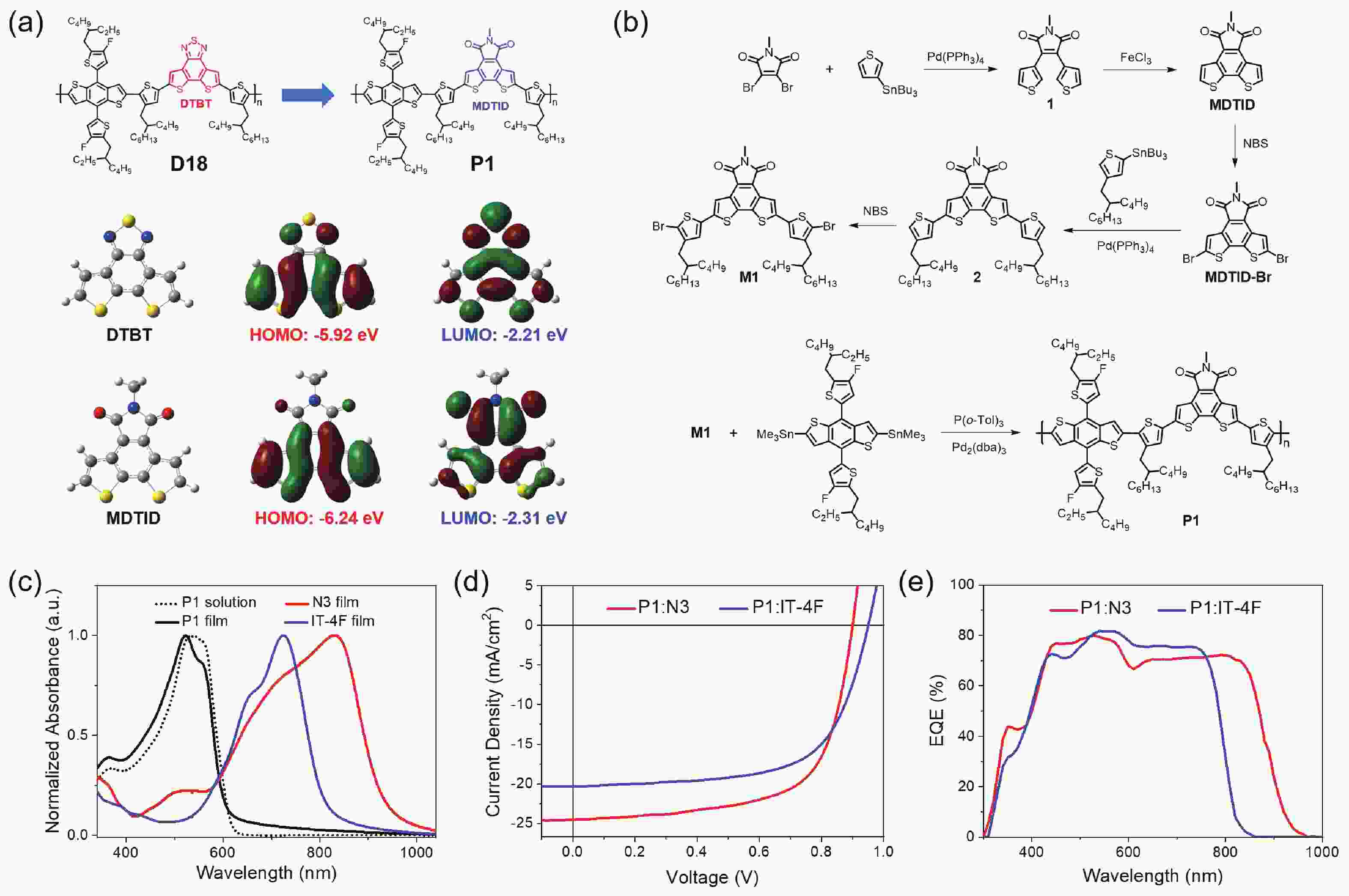

Large-area perovskite solar cell modules efficiency remains lower than small-area devices, perovskite crystallization between small and large areas difference could be one reason. Previously, diluted solution was often used to reduce viscosity to achieve uniform perovskite thin films, but this approach could narrow the crystallization window and leave insufficient time for controlled crystal growth. Meanwhile, insufficient solute supply often results in interrupted material availability for grain growth, leading to the formation of excessive small crystal nuclei and thus poor thin-film quality. Here, we developed a strategy that use a bi-functional group additive to stabilize the δ-FAPbI3 intermediate phase, which delays the direct and rapid conversion of lead iodide into α-FAPbI3 during large-area perovskite film growth. Based on this strategy, the efficiencies of perovskite modules with aperture areas of 14.6, 70.5, and 285.6 cm2 developed in this work are 24.4% (certified steady-state efficiency: 24.4%), 23.1%, and 22.4%, respectively. The efficiency loss per order-of-magnitude increase in area was reduced from 2.0% to 1.3%, which is approaching the state of the art of traditional thin-film CdTe solar cells (0.8%). In addition, the large-area module (155 cm2) retained 86% of its initial efficiency after 1053 h of maximum power point (MPP) tracking.

Robotic computing systems play an important role in enabling intelligent robotic tasks through intelligent algorithms and supporting hardware. In recent years, the evolution of robotic algorithms indicates a roadmap from traditional robotics to hierarchical and end-to-end models. This algorithmic advancement poses a critical challenge in achieving balanced system-wide performance. Therefore, algorithm-hardware co-design has emerged as the primary methodology, which analyzes algorithm behaviors on hardware to identify common computational properties. These properties can motivate algorithm optimization to reduce computational complexity and hardware innovation from architecture to circuit for high performance and high energy efficiency. We then reviewed recent works on robotic and embodied AI algorithms and computing hardware to demonstrate this algorithm-hardware co-design methodology. In the end, we discuss future research opportunities by answering two questions: (1) how to adapt the computing platforms to the rapid evolution of embodied AI algorithms, and (2) how to transform the potential of emerging hardware innovations into end-to-end inference improvements.

The computational cost of TCAD simulations is becoming prohibitively high with the complexity of advanced process technologies, making simulation acceleration a critical research priority. While end-to-end surrogate models mapping process recipes to device structures and characteristics offer a promising alternative, their application is often limited by poor generalizability and explainability. In this work, we present MPNet, a modular deep learning surrogate modeling framework for process TCAD. MPNet comprises distinct surrogate models for individual process modules, which are assembled into an integrated framework. These modular models employ a novel UNet-attention feature evolution method to capture the complex evolutions of device geometry and doping profiles. Each module can be trained separately on its individual process, after which the modules are cascaded and jointly fine-tuned to minimize error accumulation throughout the cascade. The efficacy of the proposed MPNet framework is demonstrated through a MOSFET integrated process TCAD case study. Results show that MPNet achieves a computational speedup of over 103 times compared to conventional TCAD, while maintaining predictive fidelity exceeding 98%. Finally, to illustrated the application of the proposed framework, MPNet is coupled with a PSO algorithm, showcasing its utility for fast process optimization to meet specific process targets.

Chemical mechanical polishing (CMP) serves as an indispensable process for achieving global planarization in semiconductor manufacturing, especially as integrated circuit (IC) technology advances to sub-7 nm nodes, where atomic-level surface flatness becomes crucial. Silica abrasives, which account for over 90% of the abrasive market in advanced CMP processes, operate not through simple mechanical grinding but through a key "chemical-mechanical synergistic" mechanism: chemically softening the wafer surface, then mechanically removing the softened layer to expose a new surface, which is further softened and removed, repeating this cycle to produce a smooth wafer. Despite their prevalence, conventional silica abrasives still face challenges, including relatively low material removal rate (MRR), a tendency to agglomerate, leading to poor dispersion and surface defects, and limitations in achieving ultimate surface uniformity. Significant progress has been made to address these issues. Development has progressed from simple spherical particles to complex structural designs (such as mesoporous, hollow, and raspberry-shaped structures) to enhance slurry transport and mechanical action. Surface chemical modifications (e.g., using amino or polymer groups) can improve dispersion stability and reduce scratching. Furthermore, composites with other materials (e.g., ceria, polymers) and precise control of particle size distribution are key to enhancing performance. These innovative approaches have yielded significant performance gains. State-of-the-art slurries have demonstrated the ability to achieve surface roughness below 0.1 nm RMS. The development of silica abrasives is increasingly focused on sustainability and smart manufacturing. A prominent direction is the design of biodegradable abrasives that disintegrate after use, thereby simplifying post-chemical mechanical polishing (CMP) cleanup and minimizing environmental impact—an approach fully aligned with green manufacturing principles. This review systematically summarizes the progress of silica abrasives for CMP over the past 60 years. This summary provides theoretical insights and forward-looking strategies to overcome the current limitations of abrasive technology. We believe this review will be helpful in advancing the field of CMP abrasives towards next-generation semiconductor manufacturing.